“Unfortunately, the audience was highly skeptical of my talk.” That is how Hiroo Kinoshita remembered presenting the first extreme ultraviolet images to a Japanese optics society in 1986, in an account published by ASML. He did not change his mind. It took about three more decades for the rest of the industry to come round.
Picking a wavelength
Chipmakers shrink transistors by using shorter light. ASML says that when it was founded in 1984 the industry worked with mercury-vapor lamps. Early EUV researchers tried wavelengths from 4 to 40 nanometers and settled on 13.5, the sweet spot for light made from tin plasma. WIRED put the gap in numbers: deep ultraviolet, the previous method, uses 193 nanometers.
In the 1990s a consortium including Intel, Motorola and AMD started studying EUV as lithography’s next step, WIRED reported. ASML joined in 1999, teaming up with the American group.
A hard machine to build
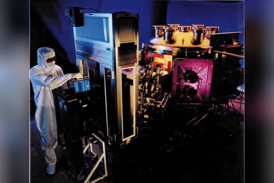
Light at 13.5 nanometers is absorbed by almost everything, so the whole system runs in a high vacuum. Lenses absorb it as well, which is why the machine bounces the beam off extremely precise mirrors. The light source fires lasers at tin droplets 50,000 times per second. Getting a full-scale source to 250 W was the main obstacle, ASML said, and once it got there, factory throughput reached 125 wafers per hour.
The milestones came slowly. Prototypes reached imec in Belgium and SUNY in Albany, New York, in 2006, and SUNY produced the first full-field EUV test chips in the spring of 2008. In 2010 ASML shipped a pre-production machine, the NXE:3100, to a Samsung research facility in South Korea, where it reached first light on Christmas Eve. Customers still could not use it to make products. “The machine basics were there, but we struggled to achieve the productivity that our customers needed,” said Jos Benschop, a senior ASML executive.
Intel, Samsung and TSMC agreed in 2012 to help fund ASML’s EUV research over five years, taking stakes in the company in return. A year later ASML shipped its first production system, the NXE:3300.
Into a phone, then to scale
Samsung’s Galaxy Note10 and Note10+ smartphones, released in 2019, were the first commercial products built with EUV. ASML shipped its 100th EUV system in December 2020, and by the end of 2021 there were 127 of its latest-generation machines at customer sites.
The price tag is steep. According to WIRED, each machine is about the size of a bus, costs $150 million and contains 100,000 parts. Most go to TSMC, Samsung and Intel. WIRED also reported that the US pushed the Dutch government to withhold the export licenses needed to send the machines to China, and that ASML says it has shipped none there.
Chip analyst David Kanter was blunt about the effort. “It’s a mere 20 years late and 10X over budget,” he told WIRED. “But if you want to build very dense structures, it’s the only tool you’ve got.”
What comes next
ASML is raising the numerical aperture of its machines from 0.33 to 0.55. WIRED reported that current machines print features at a resolution of 13 nanometers, and the High-NA generation should reach 8 nanometers. ASML’s chief technology officer, Martin van den Brink, rejects the idea that Moore’s law is dying. He prefers to call it an “illusion,” and told WIRED he expects High-NA EUV to keep driving progress for at least another 10 years.
Sources
- Making EUV: from lab to fab – ASML Stories (ASML company account of its own history, by Sander Hofman)
- The $150 Million Machine Keeping Moore's Law Alive – WIRED (Will Knight)