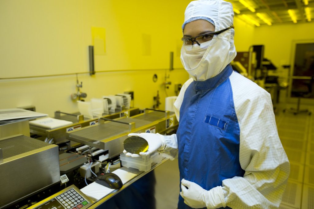
A fab that cost about $4 million in the late 1960s and early 1970s, roughly $31 million in 2024 dollars, now runs $10-$20 billion or more. Construction Physics writer Brian Potter notes that Intel is building a pair of fabs in Arizona projected at $15 billion apiece, and Samsung’s plant in Taylor, Texas at $25 billion. The money buys a factory that turns bare silicon into chips over weeks, sometimes months.
How long it takes
The Semiconductor Industry Association put numbers on the clock. Making a finished wafer, the cycle time, takes about 12 weeks on average and can stretch to 14-20 weeks for advanced processes. Assembly, test and packaging add another 6 weeks. From the day a customer places an order to delivery, the wait can reach 26 weeks.
The reason is the sheer count of operations. The association says wafer manufacturing alone can involve up to 1,400 process steps, each needing sophisticated tools. Early integrated circuits got by with five to ten masks. A leading-edge chip may need 80 or more, plus thousands of separate steps.
Four moves, repeated
Potter breaks the work into four operations: layering, patterning, doping and heat-treating. Everything starts with a wafer of extremely pure silicon, and the chip is built one layer at a time. The method, called the planar process, was invented at Fairchild Semiconductor in 1959 by Jean Hoerni.
Layering lays down films of material, using techniques such as thermal oxidation, chemical vapor deposition and sputtering. Patterning uses photolithography. The wafer gets a coat of light-sensitive photoresist, light is shone through a mask carrying the pattern, and a corrosive chemical then etches away the exposed material. One mask holds the pattern for a single chip, yet a wafer carries hundreds.
Doping, now mostly done by ion implantation, fires a beam of ions into the wafer. That damages the silicon crystal. Thermal lamps heat the wafer to over 1,000 degrees in seconds, then it cools slowly to repair the structure.
Cleaning runs through all of it. A wafer in a modern fab might be cleaned 200 times or more, since one stray particle can ruin a chip. After the last step, the wafer is cut into individual chips, wired up and encased in a protective coating.
Inside the fab
The scale of the plant explains the price. A modern logic fab might turn out 40 to 50,000 wafers a month, and a memory fab 120,000. That takes 1,000 or more tools. A handful of makers supply them, among them ASML, Lam Research, Applied Materials and Tokyo Electron. Major machines cost $5-$10 million, some more than $100 million, and ASML’s cutting-edge photolithography machines cost nearly $400 million.
Cleanrooms are built to Class 10 or Class 100 standards, allowing at most 10 or 100 particles of 0.5 microns or larger per cubic foot of air. An ordinary house has on the order of 500,000. Instead of purifying every cubic foot, fabs seal wafers inside FOUPs, front opening unified pods, which ride a ceiling-mounted rail system between tools. A TSMC fab, Potter writes, has a Class 100 cleanroom but handles its wafers in Class 0.1 mini-environments. Pods waiting in storage are flushed with nitrogen now and then to keep contaminants away.
Sources
- How to Build a $20 Billion Semiconductor Fab – Construction Physics (Brian Potter)
- Chipmakers Are Ramping Up Production to Address Semiconductor Shortage. Here's Why that Takes Time – Semiconductor Industry Association (Falan Yinug), republished by Texas Semiconductor Technologies