SANTA CLARA, CALIF., October 27, 2026 — Applied Materials is increasing its investment in BE Semiconductor Industries to approximately 20 percent of outstanding shares, a move that signals a decisive pivot toward controlling the assembly technologies required for next-generation AI chip performance. The share purchase, which builds on an initial investment made in April 2025, reinforces a strategic partnership that has evolved significantly since 2020.
The Strategic Shift Toward Advanced Packaging
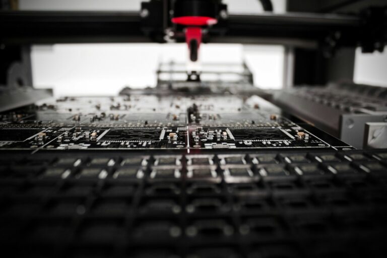
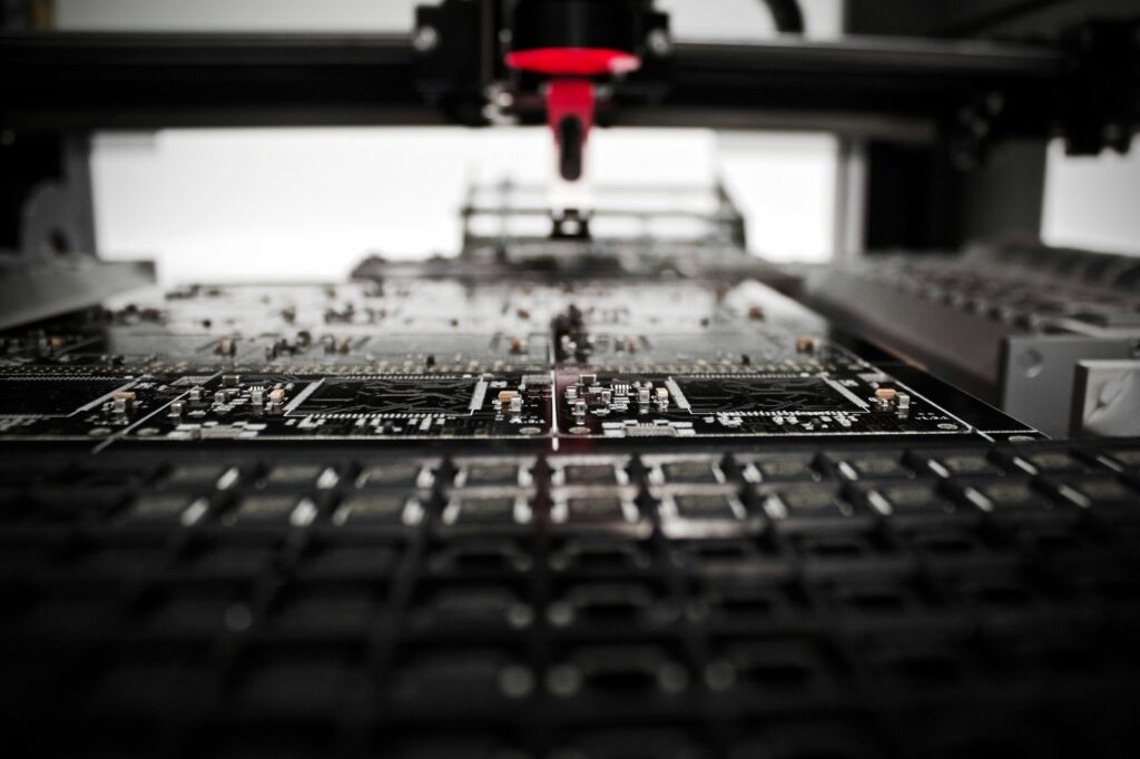
For decades, the semiconductor industry’s scaling roadmap has relied on shrinking transistor dimensions. As physical limits approach, the technical reality is that performance gains are increasingly dependent on how chips are stacked and connected. Applied Materials, the world’s second-largest semiconductor equipment supplier by revenue behind Dutch company ASML, is positioning itself at the center of this transition. By deepening its stake in Besi, a leading manufacturer of assembly equipment, Applied is moving beyond its traditional core of deposition and etch tools to secure a foothold in the critical assembly phase of chip manufacturing.
This is not a minor financial adjustment. The investment represents a substantial increase in ownership, moving from a minority position to a roughly one-fifth stake in Besi. According to the announcement, Applied Materials views this investment as long-term. The company has explicitly stated it does not intend to seek board representation at Besi, nor does it plan to increase its stake beyond approximately 20 percent. This restraint suggests a focus on technical alignment rather than corporate control, allowing both firms to operate independently while sharing a common technological trajectory.
Under the hood, this move reflects a broader industry consensus that advanced packaging is the new frontier. As AI systems demand more compute power within constrained physical envelopes, the ability to integrate logic and memory in three dimensions becomes the primary lever for efficiency. By tying its equity position to Besi, Applied is signaling that it sees hybrid bonding and related interconnect technologies not as niche applications, but as the backbone of future scaling. The detail that matters here is the shift from selling tools that build individual dies to providing the infrastructure that binds them into high-performance modules.
How Hybrid Bonding Enables Energy-Efficient AI Compute
Hybrid bonding is the technical linchpin of this strategy. Traditional wire bonding, which uses thin metal wires to connect chips, is reaching its limits in terms of speed and power efficiency. Hybrid bonding, by contrast, connects dies directly at the atomic or molecular level, eliminating the need for wires and reducing the distance electrical signals must travel. This reduction in interconnect length directly translates to lower latency and significantly reduced energy consumption, a critical factor for data centers where power costs and heat management are paramount.
Dr. Prabu Raja, President of the Semiconductor Products Group at Applied Materials, noted that hybrid bonding technology and next-generation interconnect architectures are becoming increasingly critical enablers of energy-efficient AI compute performance. The partnership extends co-innovation beyond basic hybrid bonding into new interconnect architectures and applications that support the semiconductor industry’s AI-driven scaling roadmap. This includes next-generation 3D IC scaling, logic and memory integration, and the scaling of thermo-compression bonding.
The collaboration also covers new die-on-wafer, die-on-die, and die-on-panel integration platforms. These platforms are essential for creating complex chiplets that can be combined to form larger, more powerful processors. By working closely with Besi, Applied is ensuring that its deposition and metrology tools are compatible with the precision required for these advanced bonding processes. The technical alignment is not just about selling equipment; it is about defining the standards and specifications that will govern the next generation of AI hardware. As ever, the companies that control the foundational assembly techniques will hold significant influence over the entire supply chain.
Evolution of the Partnership from 2020 to the EPIC Center
The relationship between Applied Materials and Besi did not begin with this latest investment. The companies have maintained a strategic collaboration since 2020, a period that coincided with the early emergence of AI as a dominant driver of semiconductor demand. That initial collaboration has recently expanded with Besi joining Applied Materials’ EPIC Center as an Innovation Partner. The EPIC Center serves as a hub for co-innovation, allowing both companies to test and refine new technologies in a shared environment.
This evolution from a general strategic collaboration to a formalized innovation partnership reflects the increasing complexity of advanced packaging. The expanded partnership focuses on areas that were previously siloed within individual companies. By integrating Besi’s assembly expertise with Applied’s process control and deposition capabilities, the two firms are creating a more holistic solution for chipmakers. This is particularly relevant as customers seek to reduce the time and cost associated with bringing new AI chips to market.
The initial investment in April 2025 laid the groundwork for this deepened engagement. By increasing the stake to approximately 20 percent, Applied is reinforcing the commitment made at that time. The move underscores the importance of long-term technical alignment in an industry where R&D cycles are long and capital expenditures are immense. The partnership is not a short-term financial play but a structural adjustment to the way semiconductor equipment is developed and deployed.
Implications for the Semiconductor Industry’s Scaling Roadmap
The implications of this deal extend beyond the two companies involved. For the broader semiconductor industry, it signals that the scaling roadmap is shifting from a purely lithography-driven model to one that heavily relies on advanced packaging. As leading-edge logic and DRAM fabs run at full capacity, the bottleneck is no longer just the ability to print smaller transistors, but the ability to assemble them into functional systems. Applied Materials’ management has noted that customer demand for tool deliveries has risen due to workarounds for clean room space shortages, indicating that manufacturers are aggressively investing in capacity expansion.
By securing a significant stake in Besi, Applied is positioning itself to benefit from this expansion. The company’s record revenue for fiscal Q3 2026, with growth accelerating to 24.8% compared to the same quarter a year earlier, reflects the strength of this demand. However, the investment in Besi suggests that Applied is looking beyond immediate revenue growth to secure its long-term relevance in a market where packaging is becoming as important as fabrication. The technical reality is that without advanced packaging, the performance gains from smaller transistors would be limited by I/O bottlenecks and power constraints.
This move also has competitive implications. ASML, the largest semiconductor equipment supplier, has its own strategies for advanced packaging, but Applied’s deepening tie to Besi gives it a unique advantage in the assembly segment. By controlling the tools that bond chips together, Applied can influence the design of future AI accelerators. This is a strategic play that could reshape the competitive dynamics in the equipment market, particularly as AI workloads continue to grow in complexity and scale.
Long-Term Capital Allocation and Market Positioning
From a financial perspective, the investment in Besi is a statement of confidence in the long-term viability of advanced packaging. Applied Materials has historically been a capital-efficient company, with an operating margin of 31.1% over the last twelve months, compared with 18.5% for the S&P 500. The decision to allocate capital to a strategic investment rather than a dividend or buyback reflects a belief that the returns from controlling key assembly technologies will outweigh the immediate cash flow benefits.
The share purchase is subject to regulatory review under the Hart-Scott-Rodino Antitrust Improvements Act of 1976, as amended. This is a standard procedural step for transactions of this size in the United States. The fact that Applied has entered into an accelerated share purchase agreement suggests that it is eager to finalize the deal, likely to solidify the strategic partnership before competitors can react. The regulatory process is expected to be routine, given the complementary nature of the two companies’ businesses.
For investors, the move adds a layer of complexity to Applied’s valuation. The stock has traded at a premium to the market, with a price-to-earnings ratio of 34.7 times compared to 23.0 times for the S&P 500. This premium reflects the market’s belief in Applied’s ability to sustain its recent growth rate. The investment in Besi is likely to be viewed as a positive, as it reinforces the company’s position in a high-growth segment of the semiconductor industry. However, it also ties Applied’s fortunes more closely to the success of advanced packaging, a technology that is still maturing. As ever, the detail that matters is whether the technical promise of hybrid bonding can be translated into consistent, scalable commercial success. The next few years will provide the answer, but for now, Applied is betting heavily on the future of AI compute.
Sources
- Applied Materials
- Two Reasons To Rethink Applied Materials Stock Now
- Applied Materials to Increase its Strategic Investment in BE Semiconductor Industries
Photo: Louis Reed / Unsplash (Unsplash License)