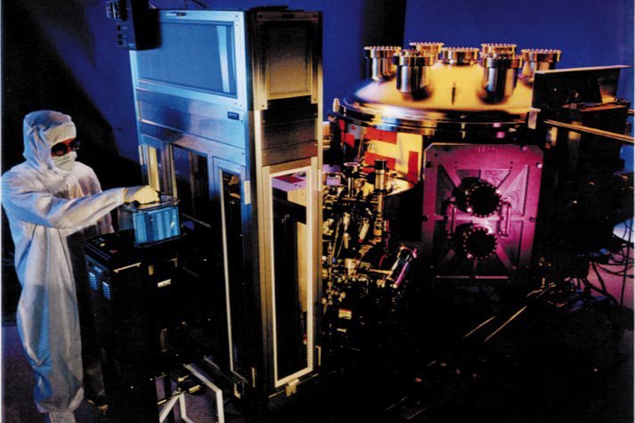
VELDHOVEN, July 13 — The machines that print the world’s most advanced chips cost more than $150 million each and rely on a Dutch company that, until a decade ago, most people had never heard of. The mechanics here are worth dissecting. Semiconductor fabrication is not a single process but a chain of over 1,000 steps, beginning with a silicon wafer sliced from a single crystal ingot.
The critical operation, photolithography, was developed at Bell Labs in the 1950s and uses ultraviolet light to etch circuit patterns onto the wafer. But the industry’s relentless push for smaller, faster transistors — nodes below 7 nanometers — has pushed that technique to its physical limits.
Enter extreme ultraviolet lithography, or EUV. First commercialized in 2018 by Dutch firm ASML, founded in 1984, EUV machines are the bottleneck for every major chipmaker today. Each unit costs over $150 million.
There is no alternative for the most advanced chips.
The supply chain trap
The catch is that even the cleanest cleanroom — these facilities boast air 10,000 times cleaner than a hospital operating room — cannot solve a raw materials problem. A single chip may contain billions of transistors; Apple’s M1 Ultra chip, released in 2022, packs 114 billion of them. Those transistors are built through doping, etching, and deposition, adding impurities to silicon, removing material, and laying down thin films.
But the supply chain for one critical input is fragile. Neon, a rare gas used in the lithography lasers, draws 40% of its global supply from Ukraine.
That supply was disrupted by the 2022 Russian invasion. On closer reading, the entire fabrication timeline — 12 to 20 weeks from start to finished chip — is vulnerable to a single missing gas.
Follow the materials
Silicon comes from sand. Copper wires connect the transistors. But it is the rare gases and the Dutch lithography machines that form the real chokepoint.
ASML holds an effective monopoly on EUV, and each new fab requires dozens of these machines. The cost of entry is astronomical, which is why only a handful of companies can afford to play.
The process itself is a marvel of precision. Wafers move through hundreds of tools in rooms where a single dust particle can ruin an entire batch. The entire operation, from raw silicon to packaged chip, takes 12 to 20 weeks.
That is a long time for an industry that turns over product cycles in months. What to watch next: the race to secure neon supplies, and whether ASML can maintain its grip on EUV as geopolitical pressure mounts.
The mechanics of chipmaking have never been more strategic — or more exposed.
Sources
{“@context”: “https://schema.org”, “@type”: “NewsArticle”, “headline”: “From Wafer to Microchip: The 1,000-Step Process Explained”, “description”: “VELDHOVEN, July 13 — The machines that print the world’s most advanced chips cost more than $150 million each and rely on a Dutch company…”, “datePublished”: “2026-07-13T09:30:00+00:00”, “author”: {“@type”: “Person”, “name”: “Beatrice Ferrari”}, “publisher”: {“@type”: “Organization”, “name”: “InfoPulse Today”, “url”: “https://newsfeed.infopulsetoday.com/”}, “citation”: [{“@type”: “CreativeWork”, “url”: “https://en.wikipedia.org/wiki/Semiconductor_device_fabrication”}]}