AMSTERDAM, October 8 — The shift is clear: extreme ultraviolet lithography has moved from experimental promise to the backbone of advanced chipmaking, enabling the industry to keep pushing transistor density in line with Moore’s Law as conventional optical methods hit their physical limits. This milestone reflects over two decades of coordinated effort, beginning with the formation of EUV LLC in 2001 by Intel, Samsung, and TSMC to jointly fund research into a solution for the diffraction barrier that threatened to halt scaling below the 10-nanometer node.
The breakthrough came with the adoption of light at a 13.5-nanometer wavelength, a choice that required entirely new approaches to optics, light sources, and vacuum systems. ASML Holding NV of the Netherlands emerged as the sole developer and supplier of EUV lithography systems after years of technical hurdles.
Its first commercial scanner, the NXE:3100, was delivered in 2010, but early models struggled with insufficient source power, low wafer throughput, and high defect rates, which limited their use in high-volume production. By 2016, ASML achieved a turning point with the NXE:3300B, delivering the reliability and performance needed for pilot lines at Samsung and TSMC. The following year, Samsung began commercial production using EUV for its 10-nanometer-class process, and TSMC followed with risk production of 7-nanometer chips in 2018.
By 2019, both foundries had moved EUV into full high-volume manufacturing for 7-nanometer logic chips, proving the technology’s readiness for mass deployment. One of the most significant impacts of EUV has been the reduction in patterning steps.
Where deep ultraviolet lithography required multiple patterning to achieve fine features, EUV’s shorter wavelength allows critical layers to be printed in a single step. This was demonstrated in TSMC’s 7-nanometer process, where EUV replaced complex DUV-based workflows, improving yield and simplifying manufacturing. The technology’s role has only grown since.
Subsequent nodes — including TSMC’s 5-nanometer in 2020, 3-nanometer in 2022, and Samsung’s 3-nanometer gate-all-around design also in 2022 — have relied on EUV for their most critical layers. In 2023, ASML delivered the first high-numerical-aperture EUV prototype to Intel, TSMC, and Samsung, targeting development for the 2-nanometer node and beyond. As of 2024, EUV lithography is regarded as essential for manufacturing logic chips at five nanometers and smaller, with more than one hundred systems shipped worldwide.
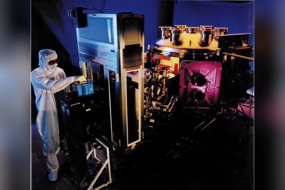
The systems depend on some of the most advanced engineering in modern production: laser-generated plasma sources, ultra-precise mirrors coated with molybdenum-silicon multilayers, and operation in high-vacuum environments to maintain beam integrity. Watch this space — the next evolution in EUV power and precision will determine how far the industry can extend scaling, and what new architectures become possible at the edge of atomic-scale fabrication.