NEW YORK, Aug 6 — The story of modern memory is, under the hood, the story of a good idea being shrunk very small for a very long time. The idea in question is Dennard scaling, named for the American engineer Robert Dennard, who invented the first DRAM in 1968. Six decades on, the industry that grew from that invention is running into a wall made of individual atoms — and the echo of that collision is the current memory shortage.
Dennard’s invention gave computing a fast, cheap way to hold data in silicon. But the device introduced in 1968 was only the opening move.
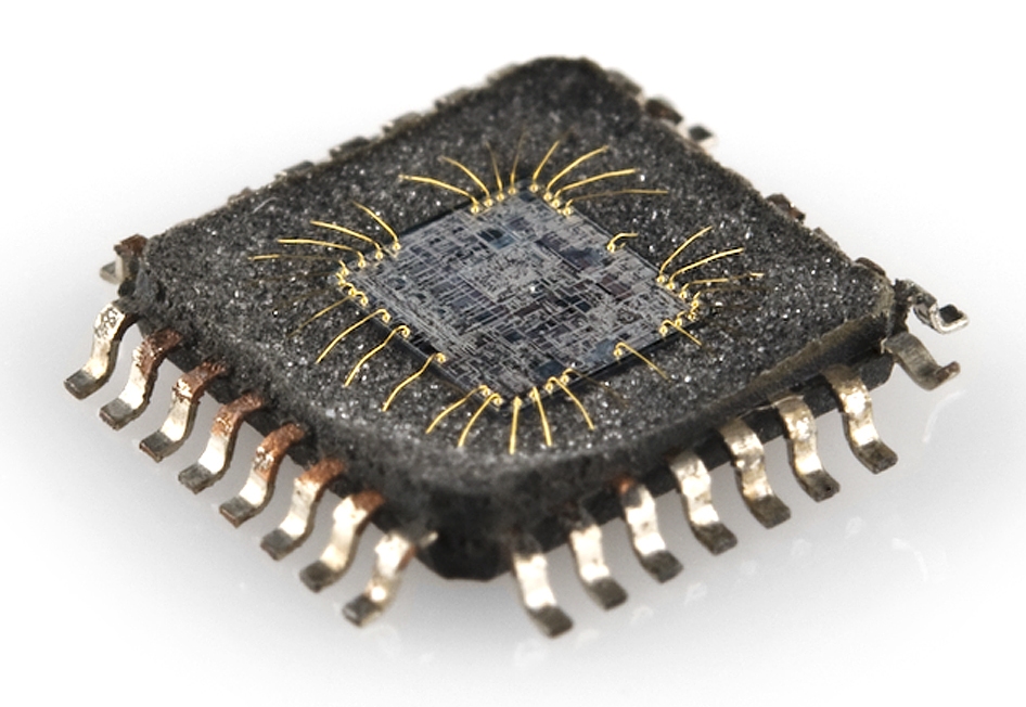
The scaling that followed — the reduction in transistor size and the increase in the density with which transistors are packed onto a chip — is what turned DRAM from a laboratory curiosity into the workhorse of every machine that computes. The numbers tell the story better than any marketing copy. The first commercial DRAM reached the market in 1971 with a capacity of 1 kilobit.
By 2022, the average DRAM density had climbed past 16 gigabits per chip. The units alone do the arithmetic; no further commentary is required.
Each shrink made those chips smaller, faster and more efficient, and that, as ever, was the deal Dennard scaling struck with the industry. Smaller transistors meant more of them per chip, and more of them per chip meant more memory per dollar. For decades, the industry simply had to keep scaling to keep delivering.
The atomic wall
The fine print in that deal is now impossible to ignore. As ever, the detail that matters is physical: transistors are approaching the size of individual atoms. At that scale, the old rules stop cooperating — the clean, predictable shrink that defined DRAM’s trajectory becomes increasingly challenging, and eventually stops being a strategy at all.
That is the technical reality behind the shortage. Memory makers can no longer simply shrink their way to more supply, and the market feels the difference.
When the scaling engine slows, the capacity that used to arrive on schedule has to come from somewhere else. The consequence is a market that is tight, and a reminder of how much of the digital world rests on a single, ageing physical principle.
What to watch next
The question now is what replaces the shrink. The industry has spent decades living off Dennard scaling’s generosity; the next phase of DRAM history will be defined by whatever fills that gap, whether it comes from new materials, new architectures, or new ways of stacking what already exists. None of that is settled.
But the trajectory of the past half-century — from a single 1-kilobit chip in 1971 to more than 16 gigabits per chip in 2022 — is a reminder that the engineers who followed Dennard have a long record of finding a way. The wall is real.
So, at least so far, was the workaround.
Sources
{“@context”: “https://schema.org”, “@type”: “NewsArticle”, “headline”: “History of DRAM: From Invention to Global Shortage”, “description”: “NEW YORK, Aug 6 — The story of modern memory is, under the hood, the story of a good idea being shrunk very small for…”, “datePublished”: “2026-08-06T09:30:00+00:00”, “author”: {“@type”: “Person”, “name”: “Sebastian Smith”}, “publisher”: {“@type”: “Organization”, “name”: “InfoPulse Today”, “url”: “https://newsfeed.infopulsetoday.com/”}, “citation”: [{“@type”: “CreativeWork”, “url”: “https://en.wikipedia.org/wiki/Dennard_scaling”}]}