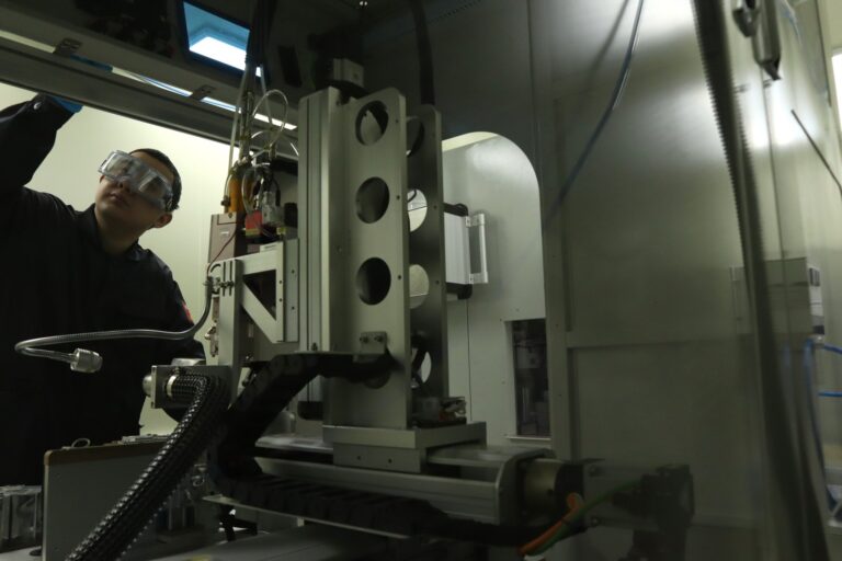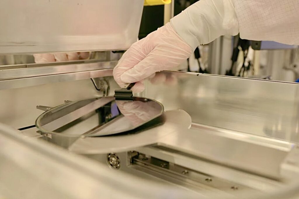
GlobalFoundries has been selected to operate two new semiconductor fabs in New York under the U.S.-Japan CHIPS initiative.
The move will generate thousands of high-skilled jobs and strengthen New York’s position in domestic chip production, according to the state’s economic development strategy.
Background of the U.S.-Japan Semiconductor Initiative
The U.S.-Japan initiative aims to strengthen domestic semiconductor production and supply chain security, as stated in the program’s framework. It is part of broader efforts to reduce reliance on overseas manufacturing and enhance resilience in critical technology sectors. The CHIPS and Science Act provides federal funding for semiconductor manufacturing in the U.S., supporting projects like this one.
Details on GlobalFoundries’ New Fabs in New York
GlobalFoundries, a major semiconductor manufacturer with existing operations in New York, was selected to operate two new fabs under the initiative. The company’s prior presence in the state includes established facilities that contribute to regional tech activity. New York’s tech sector includes growing activity in Albany’s Silicon Valley and Long Island’s research corridor, areas where semiconductor development has been expanding.
Projected Job Creation and Economic Impact
Semiconductor fabs typically create thousands of high-skilled jobs and stimulate local supplier networks, a pattern consistent with similar projects nationwide. New York has over 20 million residents and is the fourth-most populous state in the United States. New York’s economy, if it were a country, would rank as the tenth largest in the world. The state is investing in advanced manufacturing and technology sectors to drive economic growth, with officials prioritizing high-tech manufacturing through incentives and workforce development.
How the Fabs Fit Into New York’s Existing Tech Economy
New York’s existing tech economy includes established semiconductor operations and research infrastructure, particularly in upstate regions near Albany and along the Hudson Valley. The addition of two new fabs will build on this foundation, integrating with local suppliers and technical talent pools. State officials have emphasized attracting high-tech manufacturing as part of a broader strategy to modernize the industrial base and retain skilled workers.
Timeline and Next Steps for Construction and Operation
Specific dates for groundbreaking, completion, or operational launch are not provided in the available sources. The project follows the framework of the U.S.-Japan CHIPS initiative, which includes federal and state coordination for funding, permitting, and workforce training. Next steps will involve site preparation, equipment installation, and hiring, in line with standard semiconductor fab development cycles.
Significance for U.S. Chip Supply Chain Resilience
By adding domestic production capacity, the new fabs contribute to the goal of strengthening U.S. semiconductor supply chain security. The initiative reflects a strategic shift toward onshoring critical manufacturing, reducing vulnerability to global disruptions. For New York, the project reinforces its role as a hub for advanced manufacturing and aligns with state efforts to compete in the global technology economy.
Geographic and Demographic Context of New York’s Semiconductor Expansion
New York’s selection for the new semiconductor fabs aligns with its status as the fourth-most populous state in the United States, home to over 20 million residents. The state’s diverse geography includes Downstate regions centered on New York City and Long Island, which house approximately two-thirds of the population, and Upstate areas spanning the Adirondack and Catskill Mountains, the Mohawk and Hudson River valleys, and the Great Lakes region. This broad geographic footprint supports distributed economic development, with existing tech activity already concentrated in Albany’s Silicon Valley and Long Island’s research corridor.
The state’s historical development, rooted in its role as one of the original Thirteen Colonies and later amplified by infrastructure projects like the Erie Canal, has established New York as a longstanding center of economic and technological advancement. This legacy informs current efforts to attract high-tech manufacturing, including semiconductor fabrication, as part of a strategy to modernize the industrial base and leverage New York’s skilled workforce and research institutions across both urban and upstate regions.
Historical Foundations of New York’s Semiconductor Ambitions
New York’s pursuit of semiconductor manufacturing builds on a long history of technological innovation dating back to the 19th century. The state’s development of the Erie Canal in the early 1800s provided critical infrastructure that fueled its economic ascent, earning it the nickname “Empire State” as it leveraged waterways for industrial growth. This legacy of strategic infrastructure investment laid groundwork for later advancements in electronics and computing.
In the mid-20th century, New York became a hub for early computing and defense-related technology, with research institutions and manufacturing facilities emerging in regions like the Hudson Valley and Long Island. These areas cultivated a skilled workforce and technical expertise that continue to support modern semiconductor initiatives, particularly in Albany’s growing tech corridor and Long Island’s established research institutions.
The state’s historical role as a center of innovation, from colonial trade networks to 19th-century engineering projects, informs its current strategy to attract high-tech manufacturing. By situating new semiconductor fabs within this established ecosystem of research, education, and industrial capacity, New York aims to revive its legacy of technological leadership through domestic chip production.
State Incentives and Workforce Development Plans
New York is offering targeted incentives to support the new semiconductor fabs, including tax credits and grants aimed at reducing capital costs for advanced manufacturing projects. These incentives are part of the state’s broader strategy to attract high-tech investment and strengthen its position in the national chip production landscape. The state has previously used similar packages to retain and expand existing semiconductor operations in upstate regions.
Workforce development is a key component of the initiative, with plans to partner with local technical colleges and universities to train workers for high-skilled roles in fabrication, equipment maintenance, and process engineering. Programs are expected to focus on certifications in nanotechnology, materials science, and cleanroom operations, aligning with the specialized labor needs of semiconductor manufacturing. State officials have emphasized creating pipelines from community colleges to fab employment to ensure local hiring.
The initiative also includes provisions for ongoing collaboration between GlobalFoundries, state economic development agencies, and research institutions to support innovation in chip design and manufacturing processes. This coordination aims to enhance technology transfer and sustain long-term competitiveness of the new facilities within the U.S. semiconductor ecosystem.
Sources
Photo: YouTube — Purdue Engineering (CC BY 4.0)