MALTA, October 15, 2026 — GlobalFoundries will build and operate two new 300mm semiconductor fabs in Malta, New York, adding 1.8 million wafers of annual U.S. capacity and creating over 28,000 jobs through a landmark U.S.-Japan investment initiative.
Overview of GlobalFoundries’ Business and Product Focus
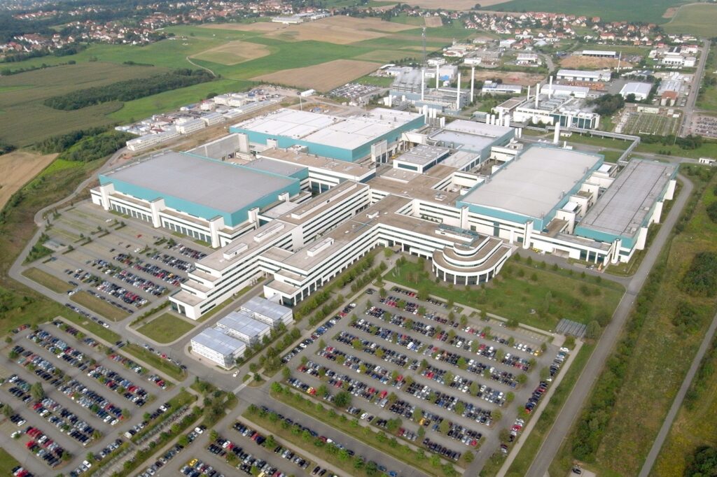
GlobalFoundries Inc. is a multinational semiconductor technology development, design and contract manufacturing company domiciled in the Cayman Islands and headquartered in Malta, New York. The company manufactures integrated circuits on wafers designed for markets such as smart mobile devices, data centers and communications infrastructure, automotive, aerospace and defense, and for consumer internet of things (IoT). As of 2023, GlobalFoundries is the third-largest semiconductor foundry by revenue. It operates one 300 mm wafer fabrication plant in Malta, New York; one 300 mm plant in Dresden, Germany; one 200 mm plant in Essex Junction, Vermont; and one 200 mm and one 300 mm plant in Singapore. GlobalFoundries is a ‘Trusted Foundry’ for the U.S. federal government and has similar designations in Singapore and Germany, including certified international Common Criteria standard (ISO 15408, CC Version 3.1).
Details of the U.S.-Japan Initiative and Funding Structure
GlobalFoundries has been selected as the technology provider and operator for two new semiconductor manufacturing facilities at its Malta, New York, site under a U.S.-Japan initiative providing up to $21 billion in funding. Enabled by President Donald J. Trump’s trade and investment agreement with Japan, the initiative will accelerate trusted semiconductor manufacturing in the United States, strengthen critical supply chains and support growing demand across automotive, industrial and connected infrastructure markets. Japan will provide the investment, while GlobalFoundries will contribute its differentiated technologies, manufacturing expertise and proven operational capabilities as technology provider and operator. An initial investment of approximately $10 billion will accelerate construction of a new 300mm semiconductor fab, expected to come online in 2029. An additional investment of approximately $10 billion would fund a second fab. GlobalFoundries has agreed with the U.S. Department of Commerce to amend its existing CHIPS and Science Act award to reallocate $955 million and accelerate investments in silicon photonics, silicon-germanium (SiGe) and advanced packaging.
Technical Specifications and Expected Output of the New Fabs
The first fab is expected to add approximately 900,000 300mm wafers of annual U.S. manufacturing capacity when fully operational. A second fab would add approximately the same amount, for a total of 1.8 million wafers annually. The facilities will produce integrated circuits on 300mm wafers for use in smart mobile devices, data centers and communications infrastructure, automotive, aerospace and defense, and consumer IoT applications. GlobalFoundries’ existing Malta site already hosts one 300mm fab, and the new facilities will expand its capacity using the same wafer size and process technologies aligned with its current product focus.
Job Creation and Economic Impact on New York’s Capital Region
The project is expected to create about 27,000 construction and ecosystem jobs and more than 1,000 high-skilled manufacturing jobs in New York’s Capital Region. The economic activity will support local suppliers, service providers and infrastructure development in the Malta area and surrounding communities. The investment reinforces New York’s role as a hub for advanced manufacturing and strengthens the state’s semiconductor ecosystem.
Strategic Significance for U.S. Semiconductor Supply Chain and National Security
The new fabs will add significant new U.S. manufacturing capacity and reinforce GlobalFoundries’ ability to support customers worldwide. As a Trusted Foundry for the U.S. federal government, the expanded capacity in Malta enhances domestic production of semiconductors for critical sectors including defense, aerospace and secure communications. The initiative strengthens supply chain resilience by reducing reliance on overseas fabrication and supports national security objectives through increased domestic output of trusted semiconductors. The reallocation of $955 million from the CHIPS and Science Act award further targets advanced packaging, silicon photonics and SiGe technologies, which are essential for next-generation computing and communication systems.
Next Steps and Timeline for Fab Construction and Operation
Construction of the first new 300mm semiconductor fab is set to begin immediately following the announcement, with site preparation and foundational work underway in Malta, New York. The facility is expected to come online in 2029, marking the completion of the initial phase of the U.S.-Japan initiative. This timeline allows for the installation of advanced manufacturing equipment, qualification of process technologies, and workforce training ahead of full-scale production.
Upon successful completion and ramp-up of the first fab, a second investment of approximately $10 billion would trigger the construction of an identical second 300mm fab at the same site. The second fab is planned to follow a similar timeline, with construction commencing after the first fab reaches operational stability and targeting completion in the early 2030s. Both facilities will be built to the same technical specifications, ensuring consistency in output and process alignment across GlobalFoundries’ expanded Malta campus.
Throughout the construction and early operation phases, GlobalFoundries will coordinate with the U.S. Department of Commerce to ensure compliance with the amended CHIPS and Science Act award, particularly regarding the accelerated investment in silicon photonics, silicon-germanium (SiGe), and advanced packaging technologies. These efforts will be integrated into the fab qualification process to support next-generation semiconductor manufacturing from the outset of operations.
Corporate History and Ownership
GlobalFoundries was born from the 2009 divestiture of AMD’s manufacturing arm, a move that turned the former AMD fab operation into an independent entity known as The Foundry Company before being rebranded as GlobalFoundries on 4 March 2009. The spin‑off was financed primarily by Mubadala Investment Company’s Advanced Technology Investment Company (ATIC), which initially secured a 65.8 % stake by purchasing AMD’s shares and assuming $1.2 billion of debt. Over the following years the company expanded its global footprint, acquiring Singapore‑based Chartered Semiconductor for US $1.8 billion in 2009 and IBM’s microelectronics business in 2014.
After a decade of private ownership, GlobalFoundries went public on the Nasdaq on 28 October 2021, pricing shares at US $47 and raising roughly US $2.6 billion. Despite the IPO, Mubadala retained a controlling interest, holding about 82 % of the outstanding shares. This ownership structure underpins the firm’s access to sovereign‑wealth capital, enabling large‑scale projects such as the new New York fabs under the U.S.–Japan initiative.
Sources
- GlobalFoundries
- GlobalFoundries selected to operate two new semiconductor fabs in New York under landmark U.S.-Japan initiative | GlobalFoundries
- GlobalFoundries selected to operate two new semiconductor fabs in New York under landmark U.S.-Japan initiative | GlobalFoundries
Photo: Fensterblick. (CC BY-SA 3.0)