TAIPEI, July 6 — The fabrication of a modern semiconductor chip, from raw sand to finished processor, can take three to six months, according to industry data. The process begins with one of the most common materials on Earth. Silicon, the second most abundant element in the Earth’s crust, is derived from sand.
It is grown into a pure crystal ingot, which is then sliced into thin wafers. Each wafer then undergoes hundreds of steps.
These steps include photolithography, doping, etching, and deposition. They build microscopic transistors onto the silicon surface. A modern chip like Apple’s A17 Bionic contains 19 billion transistors on a die roughly 100 square millimeters.
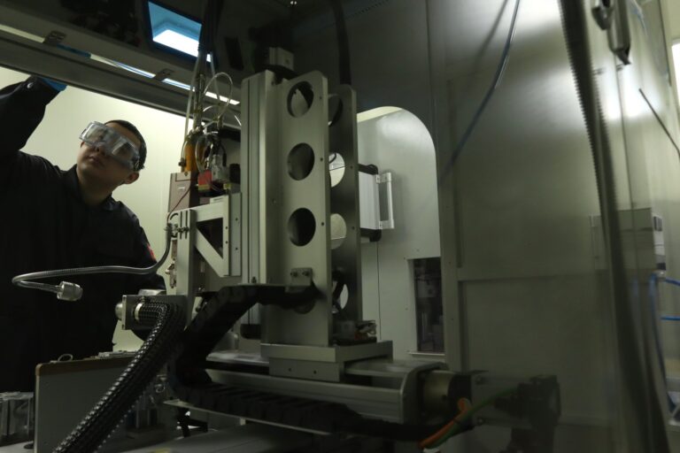
The photolithography stage is dominated by a single Dutch firm. ASML controls over 90% of the market for extreme ultraviolet (EUV) lithography machines.
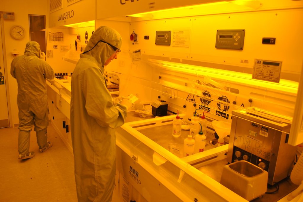
Each machine costs over $150 million. Fabrication occurs in highly automated facilities known as ‘fabs’. These plants can cost up to $20 billion to build.
An example is TSMC’s Fab 18 in Taiwan. Yield rates are critical to profitability. This figure measures the percentage of functional chips per wafer.
Leading fabs achieve yields above 90% for mature nodes. The strategic context is clear.
Taiwan, through TSMC, holds a central position in global semiconductor production. The island’s fabs produce chips for companies worldwide, including Apple. Any disruption to this supply chain would have immediate geopolitical consequences.
The concentration of advanced manufacturing in one region is a factor governments now watch closely. A single EUV machine from ASML costs more than $150 million.
The company’s near-monopoly on this critical equipment gives the Netherlands significant leverage in the technology sector. For now, the process continues. From sand to circuit, the journey takes months.
The chips that result power everything from smartphones to military systems.