SANTA CLARA, July 8 — The story of the modern world begins not with a bang, but with a sliver of germanium, no larger than a thumbnail, sitting on a lab bench in Dallas. On the ground here in Silicon Valley, where the air hums with the quiet ambition of a thousand chip startups, the integrated circuit is the invisible architecture upon which everything is built.
It is the reason a phone in a pocket holds more power than the room-sized computers of a generation ago, and the reason the global economy runs at the speed of light. The invention that made this possible did not emerge from a single flash of genius, but from two separate, competitive acts of creation, one in the autumn of 1958 and another in the spring of 1959.
Jack Kilby, an engineer at Texas Instruments—a company that traces its own origins back to 1930—stood before a room of skeptical colleagues on September 12, 1958. On that day, he demonstrated the first working integrated circuit. His device was built on germanium, a semiconductor material that was then common but would soon be eclipsed.
It was a crude, fragile thing by today’s standards, but it worked. Kilby had solved a problem that had vexed the electronics industry for years: how to cram multiple components—transistors, resistors, capacitors—onto a single piece of semiconductor material, eliminating the tangle of wires that made early computers unreliable and enormous.
It was a breakthrough that would eventually earn him the Nobel Prize in Physics in the year 2000, a recognition that came more than four decades after his initial demonstration. But Kilby’s germanium chip was not the final word. Just months later, in 1959, Robert Noyce, a co-founder of Fairchild Semiconductor—a company itself founded in 1957—developed a different approach, using silicon as the base material.
Noyce’s silicon integrated circuit solved key manufacturing and reliability problems that plagued Kilby’s germanium design. Silicon was more abundant, more stable at high temperatures, and, critically, could be oxidized to form an insulating layer that allowed for more complex circuit patterns. Noyce’s invention became the industry standard, the foundation upon which the entire semiconductor industry was built.
The two men, Kilby and Noyce, would spend years in a legal battle over patent rights, a fight that ultimately ended in a cross-licensing agreement that recognized both as essential inventors. The integrated circuit, in its final form, was a hybrid of both their visions.
The First Commercial Chip and the Law That Shaped an Industry
The first commercial integrated circuit to hit the market was the Fairchild μA702 operational amplifier, released in 1963. It was a modest device by modern reckoning, but it marked the moment the integrated circuit stepped out of the laboratory and into the real world. It found its way into military avionics, early computers, and industrial control systems.
The μA702 was a proof of concept that the integrated circuit was not just a scientific curiosity but a viable commercial product. It was the beginning of a revolution that would transform every aspect of human life.
In 1965, Gordon Moore, a chemist and physicist who would later co-found Intel, published a paper that articulated a trend that had already begun to take shape. Moore observed that the number of transistors that could be placed on an integrated circuit was doubling approximately every two years. This observation, which came to be known as Moore’s Law, was not a law of physics but a self-fulfilling prophecy, a roadmap that the entire semiconductor industry adopted as its guiding principle.
For decades, the industry kept pace with Moore’s prediction, packing ever more transistors onto ever smaller chips, driving down the cost of computing and making possible the digital age. It was a remarkable feat of collective engineering and economic coordination, a race that the industry ran—and won—for more than half a century.
The first microprocessor, the Intel 4004, was released in 1971. It contained 2,300 transistors, a number that seems laughably small today but was revolutionary at the time. The 4004 was the first time that the central processing unit of a computer—the brain of the machine—had been shrunk down to a single chip.
It was the ancestor of every modern processor, from the chips in smartphones to the massive data center servers that power the cloud. The 4004 was a demonstration that the integrated circuit could do more than just simple logic; it could be a complete, programmable computer on a single piece of silicon.
The Limits of Shrinking and the FinFET Revolution
By the early 2000s, the semiconductor industry was approaching a fundamental barrier. The planar transistor, the basic building block of integrated circuits for decades, was running out of room to shrink. As transistors got smaller, they began to leak current, consuming too much power and generating too much heat.
The industry faced a crisis: Moore’s Law seemed to be hitting a wall. The solution came in 2011, when Intel introduced a new transistor architecture called the FinFET, or fin field-effect transistor.
Instead of lying flat on the surface of the chip, the transistor’s channel was raised up into a thin fin, allowing the gate to wrap around it on three sides. This gave the gate much better control over the flow of current, reducing leakage and allowing the relentless march of miniaturization to continue. The FinFET was a breakthrough that bought the industry another decade of progress.
But even the FinFET has its limits. The current leading-edge chips, the ones that power the most advanced smartphones, servers, and artificial intelligence systems, are manufactured using a technology called extreme ultraviolet lithography, or EUV.
This technology was developed by ASML, a Dutch company that was founded in 1984. ASML began shipping its first EUV lithography machines in 2018, and since then, it has become the sole supplier of these systems. Each EUV machine costs over $150 million, a price tag that reflects the extraordinary complexity of the technology.
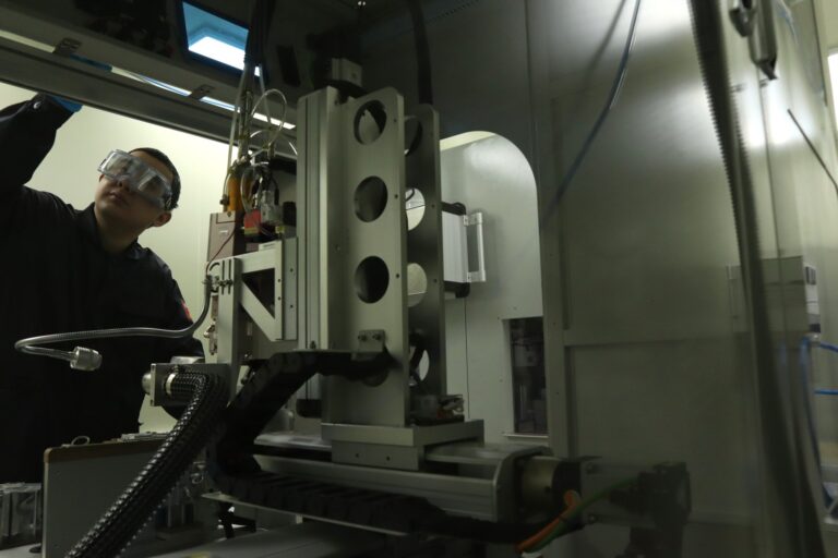
EUV uses light with a wavelength of just 13.5 nanometers, far shorter than the deep ultraviolet light used in previous generations of lithography. This allows chipmakers to pattern features that are just a few nanometers across, etching circuits onto silicon wafers with a precision that borders on the atomic. By 2023, the cumulative effect of these decades of innovation was staggering.
Advanced chips, such as Apple’s M2 Ultra, contained 134 billion transistors. That is a number so large it is almost impossible to grasp.
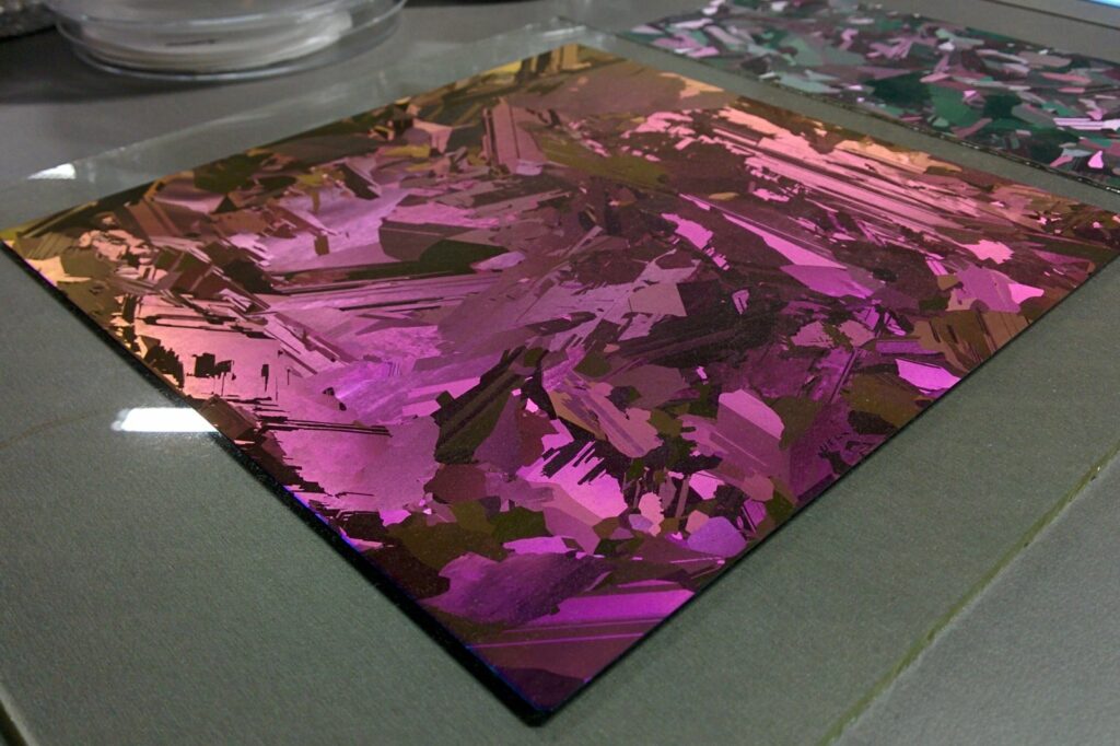
It represents a doubling of transistor count, roughly every two years, for more than five decades. The Intel 4004, with its 2,300 transistors, seems like a relic from a different age. Yet the fundamental principle remains the same: a single, tiny sliver of silicon, etched with patterns of exquisite complexity, that can perform billions of calculations per second.
The integrated circuit has become the universal machine, the substrate upon which the digital world is built.
What to Watch Next
The integrated circuit is not a finished invention. The industry is already looking beyond the FinFET, exploring new transistor designs like the gate-all-around (GAA) FET, which wraps the gate completely around the channel, offering even better control. ASML is developing next-generation EUV machines with even higher numerical aperture, capable of patterning features smaller than any current chip.
The cost of these machines is expected to rise well beyond the $150 million mark, concentrating the manufacturing of leading-edge chips in the hands of a few companies—TSMC, Samsung, and Intel itself. The geopolitics of chip manufacturing has become a central concern for governments around the world, with the United States, Europe, and Japan all investing heavily in domestic semiconductor production.
The story of the integrated circuit is a story of relentless progress, of a technology that has consistently defied predictions of its demise. It is a story of two inventors, Kilby and Noyce, whose separate creations merged into a single, world-changing technology. It is a story of a law—Moore’s Law—that was not a law at all, but a collective commitment to a future of ever-increasing capability.
And it is a story that is still being written, in the clean rooms of Taiwan, the labs of the Netherlands, and the fabrication plants of Arizona. The integrated circuit is not a finished product.
It is a living, evolving technology, and the next chapter is being written now.
{“@context”: “https://schema.org”, “@type”: “NewsArticle”, “headline”: “Semiconductor Chip’s 65-Year History: From Sand to Silicon”, “description”: “SANTA CLARA, July 8 — The story of the modern world begins not with a bang, but with a sliver of germanium, no larger than…”, “datePublished”: “2026-07-08T09:30:00+00:00”, “author”: {“@type”: “Person”, “name”: “Isabella Moore”}, “publisher”: {“@type”: “Organization”, “name”: “InfoPulse Today”, “url”: “https://newsfeed.2bme.xyz/”}}